1. Essential Characteristics and Nanoscale Actions of Silicon at the Submicron Frontier
1.1 Quantum Confinement and Electronic Structure Change
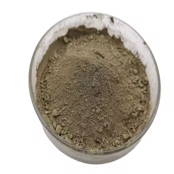
(Nano-Silicon Powder)
Nano-silicon powder, composed of silicon bits with particular dimensions listed below 100 nanometers, represents a standard change from mass silicon in both physical behavior and functional utility.
While mass silicon is an indirect bandgap semiconductor with a bandgap of roughly 1.12 eV, nano-sizing generates quantum arrest effects that basically change its digital and optical buildings.
When the fragment size methods or drops below the exciton Bohr span of silicon (~ 5 nm), charge service providers end up being spatially constrained, leading to a widening of the bandgap and the appearance of noticeable photoluminescence– a phenomenon missing in macroscopic silicon.
This size-dependent tunability allows nano-silicon to discharge light across the visible range, making it an appealing prospect for silicon-based optoelectronics, where standard silicon fails because of its inadequate radiative recombination effectiveness.
Moreover, the boosted surface-to-volume proportion at the nanoscale improves surface-related phenomena, including chemical sensitivity, catalytic task, and interaction with magnetic fields.
These quantum results are not merely academic curiosities however create the structure for next-generation applications in energy, noticing, and biomedicine.
1.2 Morphological Variety and Surface Chemistry
Nano-silicon powder can be manufactured in numerous morphologies, including round nanoparticles, nanowires, permeable nanostructures, and crystalline quantum dots, each offering distinct advantages relying on the target application.
Crystalline nano-silicon normally maintains the diamond cubic framework of mass silicon but shows a greater thickness of surface area defects and dangling bonds, which should be passivated to support the product.
Surface area functionalization– typically attained through oxidation, hydrosilylation, or ligand add-on– plays an important role in identifying colloidal security, dispersibility, and compatibility with matrices in compounds or organic environments.
For example, hydrogen-terminated nano-silicon shows high sensitivity and is susceptible to oxidation in air, whereas alkyl- or polyethylene glycol (PEG)-layered bits exhibit enhanced security and biocompatibility for biomedical usage.
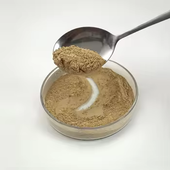
( Nano-Silicon Powder)
The existence of an indigenous oxide layer (SiOₓ) on the fragment surface area, also in marginal quantities, considerably affects electrical conductivity, lithium-ion diffusion kinetics, and interfacial reactions, specifically in battery applications.
Comprehending and controlling surface chemistry is therefore essential for taking advantage of the complete capacity of nano-silicon in sensible systems.
2. Synthesis Strategies and Scalable Manufacture Techniques
2.1 Top-Down Strategies: Milling, Etching, and Laser Ablation
The manufacturing of nano-silicon powder can be extensively classified into top-down and bottom-up techniques, each with unique scalability, purity, and morphological control characteristics.
Top-down techniques involve the physical or chemical decrease of bulk silicon into nanoscale fragments.
High-energy sphere milling is an extensively utilized industrial approach, where silicon chunks undergo extreme mechanical grinding in inert environments, resulting in micron- to nano-sized powders.
While cost-efficient and scalable, this technique commonly presents crystal flaws, contamination from crushing media, and broad particle size distributions, needing post-processing purification.
Magnesiothermic decrease of silica (SiO ₂) followed by acid leaching is one more scalable route, specifically when using natural or waste-derived silica sources such as rice husks or diatoms, providing a sustainable pathway to nano-silicon.
Laser ablation and responsive plasma etching are more accurate top-down methods, with the ability of creating high-purity nano-silicon with controlled crystallinity, though at greater cost and reduced throughput.
2.2 Bottom-Up Approaches: Gas-Phase and Solution-Phase Growth
Bottom-up synthesis allows for higher control over bit dimension, shape, and crystallinity by constructing nanostructures atom by atom.
Chemical vapor deposition (CVD) and plasma-enhanced CVD (PECVD) make it possible for the growth of nano-silicon from gaseous forerunners such as silane (SiH FOUR) or disilane (Si two H ₆), with specifications like temperature, pressure, and gas circulation dictating nucleation and growth kinetics.
These methods are specifically reliable for generating silicon nanocrystals embedded in dielectric matrices for optoelectronic devices.
Solution-phase synthesis, including colloidal courses using organosilicon substances, permits the manufacturing of monodisperse silicon quantum dots with tunable discharge wavelengths.
Thermal decomposition of silane in high-boiling solvents or supercritical liquid synthesis additionally yields high-quality nano-silicon with narrow dimension distributions, appropriate for biomedical labeling and imaging.
While bottom-up approaches normally produce exceptional material high quality, they encounter difficulties in large manufacturing and cost-efficiency, necessitating recurring research right into crossbreed and continuous-flow procedures.
3. Energy Applications: Changing Lithium-Ion and Beyond-Lithium Batteries
3.1 Duty in High-Capacity Anodes for Lithium-Ion Batteries
Among the most transformative applications of nano-silicon powder depends on power storage space, especially as an anode product in lithium-ion batteries (LIBs).
Silicon provides a theoretical certain ability of ~ 3579 mAh/g based on the development of Li ₁₅ Si ₄, which is nearly ten times greater than that of conventional graphite (372 mAh/g).
However, the large quantity development (~ 300%) throughout lithiation creates particle pulverization, loss of electric contact, and continual strong electrolyte interphase (SEI) formation, resulting in quick capacity discolor.
Nanostructuring minimizes these problems by reducing lithium diffusion paths, fitting pressure better, and minimizing fracture probability.
Nano-silicon in the kind of nanoparticles, porous structures, or yolk-shell frameworks makes it possible for reversible biking with enhanced Coulombic performance and cycle life.
Industrial battery technologies now incorporate nano-silicon blends (e.g., silicon-carbon compounds) in anodes to increase power thickness in customer electronic devices, electric cars, and grid storage systems.
3.2 Possible in Sodium-Ion, Potassium-Ion, and Solid-State Batteries
Past lithium-ion systems, nano-silicon is being checked out in emerging battery chemistries.
While silicon is much less responsive with salt than lithium, nano-sizing enhances kinetics and makes it possible for minimal Na ⁺ insertion, making it a candidate for sodium-ion battery anodes, especially when alloyed or composited with tin or antimony.
In solid-state batteries, where mechanical security at electrode-electrolyte user interfaces is vital, nano-silicon’s capability to go through plastic contortion at little scales lowers interfacial anxiety and boosts contact upkeep.
Furthermore, its compatibility with sulfide- and oxide-based solid electrolytes opens up avenues for safer, higher-energy-density storage solutions.
Research continues to maximize interface design and prelithiation techniques to optimize the durability and efficiency of nano-silicon-based electrodes.
4. Arising Frontiers in Photonics, Biomedicine, and Compound Products
4.1 Applications in Optoelectronics and Quantum Light Sources
The photoluminescent residential properties of nano-silicon have actually revitalized initiatives to create silicon-based light-emitting devices, an enduring challenge in incorporated photonics.
Unlike bulk silicon, nano-silicon quantum dots can show reliable, tunable photoluminescence in the visible to near-infrared variety, making it possible for on-chip source of lights suitable with complementary metal-oxide-semiconductor (CMOS) innovation.
These nanomaterials are being incorporated right into light-emitting diodes (LEDs), photodetectors, and waveguide-coupled emitters for optical interconnects and noticing applications.
Moreover, surface-engineered nano-silicon exhibits single-photon exhaust under certain flaw arrangements, placing it as a prospective platform for quantum information processing and safe and secure interaction.
4.2 Biomedical and Environmental Applications
In biomedicine, nano-silicon powder is getting attention as a biocompatible, biodegradable, and safe choice to heavy-metal-based quantum dots for bioimaging and medication distribution.
Surface-functionalized nano-silicon bits can be made to target particular cells, launch restorative agents in reaction to pH or enzymes, and offer real-time fluorescence monitoring.
Their destruction into silicic acid (Si(OH)FOUR), a normally happening and excretable substance, minimizes long-lasting toxicity concerns.
In addition, nano-silicon is being investigated for environmental remediation, such as photocatalytic destruction of contaminants under visible light or as a reducing agent in water treatment procedures.
In composite products, nano-silicon improves mechanical toughness, thermal security, and put on resistance when integrated right into metals, ceramics, or polymers, especially in aerospace and automobile parts.
In conclusion, nano-silicon powder stands at the junction of essential nanoscience and industrial development.
Its special mix of quantum effects, high sensitivity, and versatility throughout energy, electronic devices, and life sciences highlights its duty as a crucial enabler of next-generation technologies.
As synthesis methods development and combination obstacles are overcome, nano-silicon will certainly continue to drive progress towards higher-performance, sustainable, and multifunctional product systems.
5. Distributor
TRUNNANO is a supplier of Spherical Tungsten Powder with over 12 years of experience in nano-building energy conservation and nanotechnology development. It accepts payment via Credit Card, T/T, West Union and Paypal. Trunnano will ship the goods to customers overseas through FedEx, DHL, by air, or by sea. If you want to know more about Spherical Tungsten Powder, please feel free to contact us and send an inquiry(sales5@nanotrun.com).
Tags: Nano-Silicon Powder, Silicon Powder, Silicon
All articles and pictures are from the Internet. If there are any copyright issues, please contact us in time to delete.
Inquiry us